Photolithography Consulting
and Coaching
About Us
Photolithography.net is a company which specializes in semiconductor photolithography and all front end semiconductor optimization and troubleshooting by paid coaching and consulting. We can help with any lithography or other semiconductor issue including defect, exposure tool and coater track issues.
Collectively we have years of fab experience which includes technologies such as g-h-i-line, Krf, Arf, EUV, E-beam, registration and defect investigations. Our services can be obtained by a PO from any semiconductor company. You can contact us by calling 503-608-7611 or use our contact form. We strive to return your call or email as soon as possible. Our normal response time is within 1 hour. We are also much less expensive than hiring a new Engineer. We can provide onsite Engineering service while you look and interview candidates. We can train new engineers.
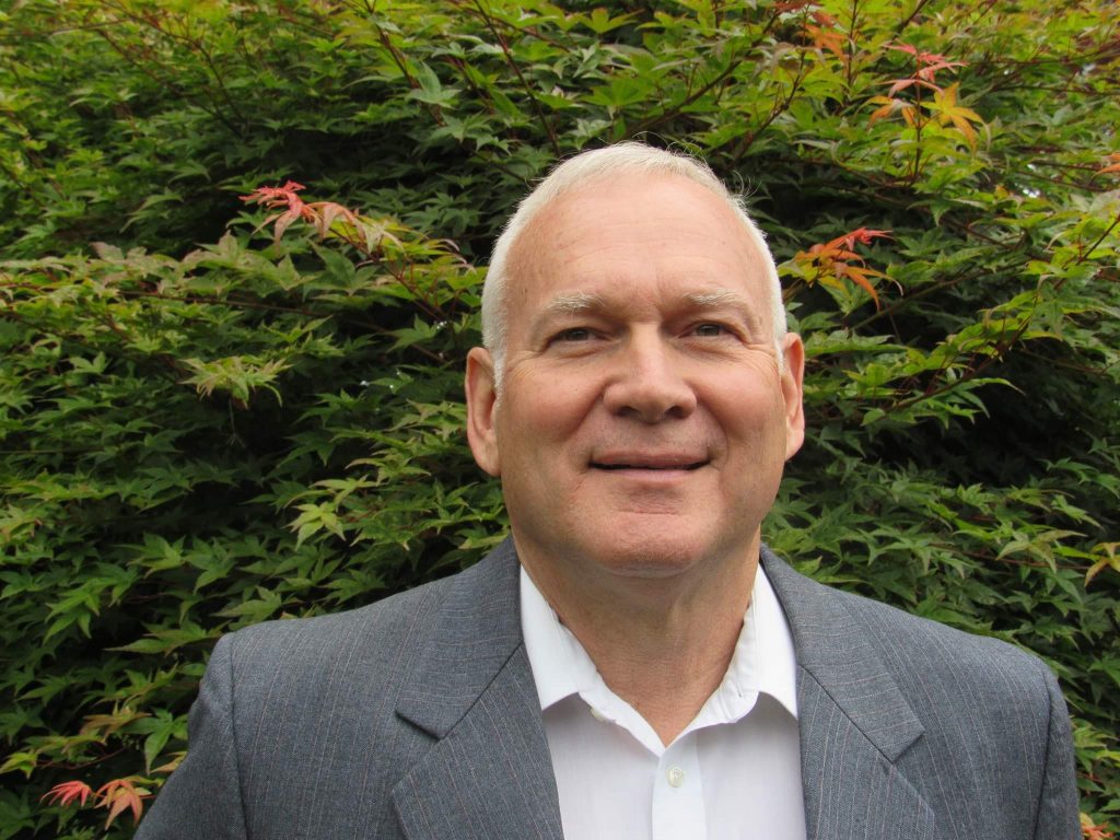
Dave White
I have 25 years as a Lithography Engineer plus 10 years consulting. Intel, then Micron, then Fujitsu then TOK Photoresist. Now Consulting for Photolithography.net. I have worked on all areas of lithography. Including ASML EUV. I have co-authored a SPIE poster paper on ArF double patterning with Dr. Tom Wallow in 2007. I am interested in helping any semiconductor company with their litho needs whether g-line or advanced litho. I have worked inside the following companies cleanrooms. Seagate hard drive head and media sites, Cypress, HGST, Polar Semi, Western Digital, Linear Tech, Texas Instruments, Intel, Freescale, SVTC, Microchip, Spansion, and Maxim. Also, The effect of resist dissolution process on pattern formation variability:
Contact Us
Please fill out the form below or call us at 503-608-7611.